
Microsanj News
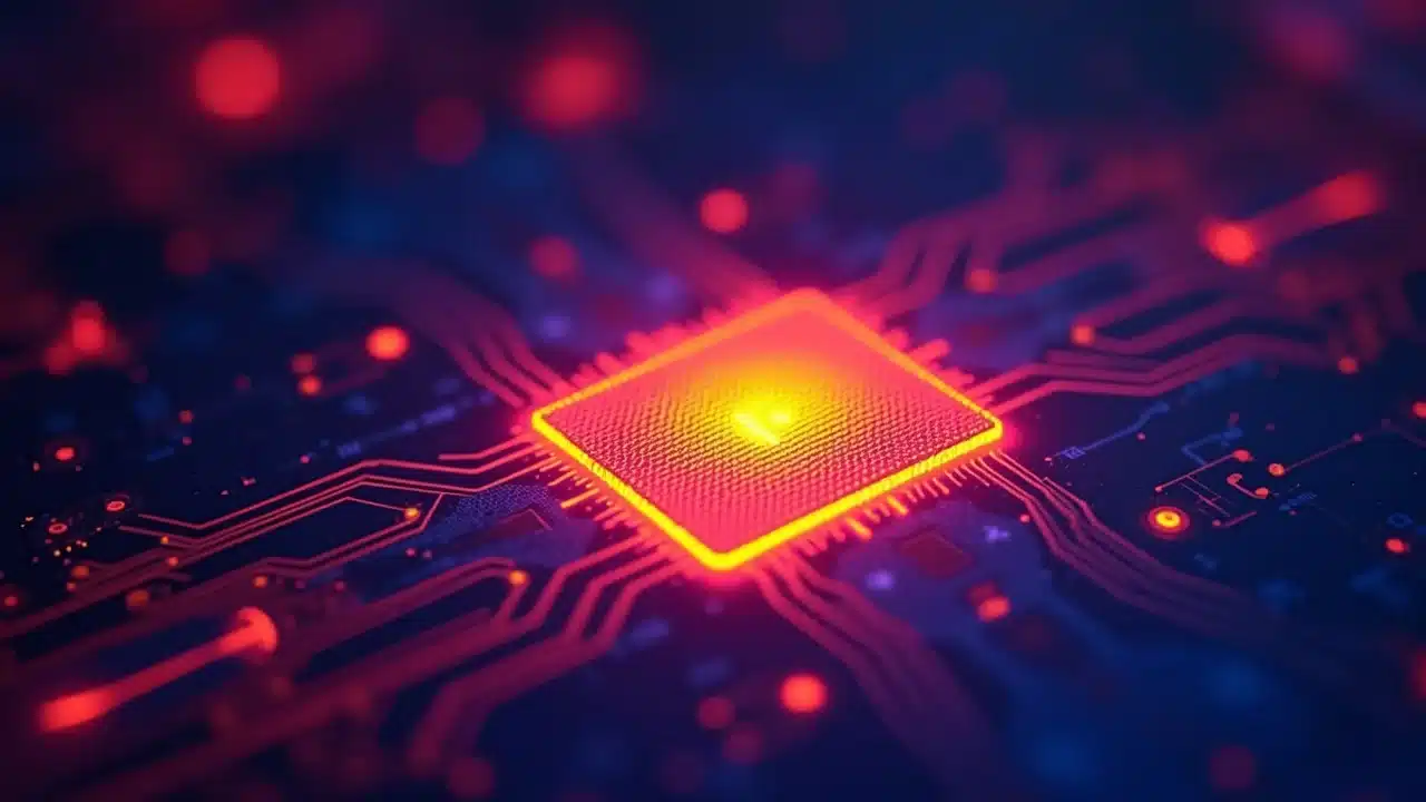
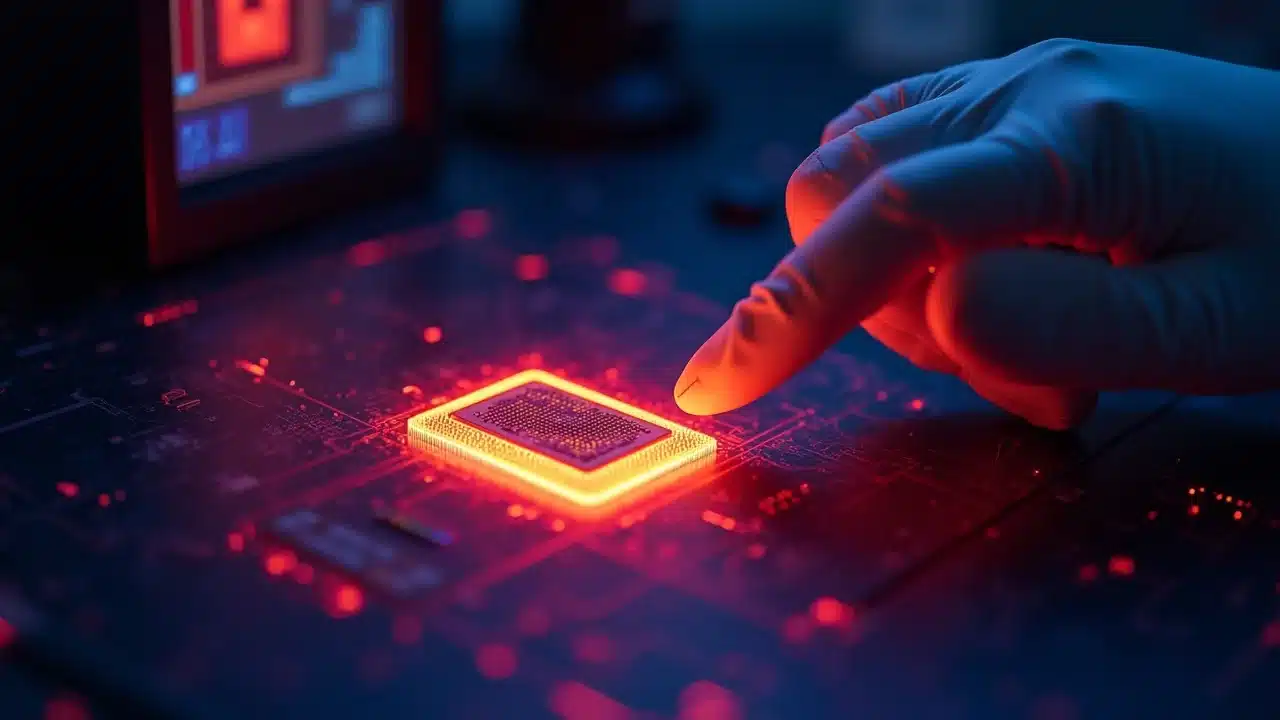
As semiconductor devices become smaller, faster, and more densely integrated, heat management has emerged as a critical challenge hardly visible to conventional tools. Traditional infrared thermal imaging methods are often inadequate to detect the sub-micron hotspots that can deteriorate device reliability in power electronics. At the forefront of solving this visibility problem is MicroSanJ LLC, whose innovative thermoreflectance imaging technology offers unparalleled insight into nanoscale thermal behavior, especially in advanced semiconductor devices showcased at the upcoming APEX Expo.
Why Thermoreflectance Reliability Semiconductor Matters More Than Ever
The evolution of semiconductor technology has pulled thermal management into the spotlight as one of the most pressing engineering bottlenecks today. Shrinking chip geometries combined with increased power densities create nanoscale thermal hotspots that traditional IR cameras simply cannot resolve. This gap in thermal visibility can lead to early device degradation and unexpected failures.
MicroSanJ’s solutions provide engineers with a powerful window into these hidden thermal phenomena through advanced thermoreflectance reliability semiconductor techniques. These allow for early detection of critical heat signatures that traditional methods often miss, enabling proactive design adjustments and improving overall device longevity.
Jonathan Thein of MicroSanJ explains, “Our systems use light—rather than emissivity-dependent IR—to visualize temperature with sub-micron spatial resolution and nanosecond to picosecond time response, making it possible to pinpoint hidden hotspots and verify thermal models. ” This capability marks a significant leap in ensuring semiconductor devices function reliably under increasingly demanding thermal loads.
Understanding Thermoreflectance Technique and Its Impact on Semiconductor Reliability
The thermoreflectance technique represents a paradigm shift in thermal analysis for semiconductor devices. Unlike conventional IR imaging that depends heavily on emissivity and offers limited resolution, thermoreflectance leverages visible and near-UV light to create thermal maps with resolutions reaching 200–300 nanometers. This unprecedented detail allows engineers to visualize thermal events localized deep within complex device architectures.
Beyond spatial resolution, the technique provides ultra-fast temporal responses — from nanoseconds down to picoseconds — enabling capture of transient thermal events critical to device function. These advances allow for more precise thermal characterizations, improving design feedback loops and helping prevent thermal failures before they occur.
Key Thermal Challenges in Modern Electronic Devices and the Role of Thermoreflectance
Highly Localized Hotspots in Advanced Nodes and Power Devices
The relentless push toward smaller fabrication nodes in semiconductor devices has introduced highly localized hotspots that are mere hundreds of nanometers wide. These hotspots result from increased power densities and compact geometries that traditional tools fail to detect. Failure to identify such hotspots early can accelerate material degradation and reduce device reliability.
Here, thermoreflectance imaging shines by revealing these nanoscale hotspots with high spatial precision, offering engineers the data needed to redesign or reinforce cooling pathways effectively, extending device lifespan and performance.
Multilayer and 3D Packaging Complexities
Emerging packaging techniques—such as chiplets integration, interposers, hybrid bonding, and 3D IC stacks—introduce intricate multilayer structures and buried interfaces that complicate heat flow. These vertical heat transport pathways are difficult to characterize through simulations or traditional thermal tools.
MicroSanJ’s thermoreflectance imaging delivers both surface and subsurface thermal insights, enabling visualization of heat dynamics across layers. This offers crucial inputs for accurate thermal management strategies in increasingly complex packaging schemes.
New Materials with Complex Thermal Properties
Semiconductor materials such as diamond heat spreaders, gallium nitride (GaN), and silicon carbide (SiC) exhibit anisotropic and interface-dependent thermal behaviors. These complex thermal properties challenge assumptions often used in thermal design.
Thermal Properties of Wide Bandgap Semiconductor Materials
Wide bandgap semiconductors like GaN and SiC are pivotal in high-power and RF electronics due to their superior switching speeds and thermal stability. However, their anisotropic thermal conductivities require precise measurement methods that provide in-situ thermal property data rather than relying on generalized models.
Thermoreflectance techniques allow measurement of thermal conductivity and interface thermal resistance in these materials, providing an accurate thermal performance picture essential for reliability.
How Thermoreflectance Technique Outperforms Traditional Thermal Imaging in Semiconductor Analysis
Sub-Micron Spatial Resolution Advantages
Conventional infrared thermal imaging is limited by long wavelengths, restricting resolution to micron-scale hotspots at best. Thermoreflectance breaks through this barrier by employing visible and near-UV light, probing thermal features at sub-micron scales (approximately 200–300 nm). This high resolution is critical for detailed thermal mapping in next-generation semiconductor devices with densely packed transistor elements.
Access to finer spatial detail allows engineers to discover thermal anomalies invisible to IR imaging, facilitating early-stage correction and enhancing overall device reliability.
Ultra-Fast Temporal Response for Transient Thermal Events
Transient thermal behaviors — rapid heating and cooling cycles occurring in nanoseconds or faster — directly influence semiconductor device reliability, especially in power electronics and high-speed RF components.
MicroSanJ’s transient thermoreflectance (TR) technology captures these fast thermal events with timing resolution down to 50 nanoseconds, while pump-probe approaches reach picosecond scales for thin-film and interface thermal characterization. This temporal precision provides a dynamic view of time-dependent heat flow rarely accessible with traditional tools.
Combined Imaging and Materials Characterization Capabilities
MicroSanJ integrates full-field thermal imaging with time-domain thermoreflectance (TDTR) for thermal property analysis within the same product family. This dual capability allows users to directly correlate device-level hotspots with the underlying materials’ thermal conductivity and interface resistance.
Jonathan Thein, of MicroSanJ, states, “Only MicroSanJ offers both full-field thermal imaging and TDTR-based materials analysis in the same product family, giving users a complete view from device-level hotspots to underlying thermal conductivity and interface resistance. ” This holistic approach bridges the gap between real device thermal behavior and material science, vital for refining semiconductor design.
Applications Driving Demand for Thermoreflectance in Semiconductor and Electronic Devices
Semiconductors and Advanced Packaging including Chiplets and 3DIC
With the rise of chiplets and 3D integrated circuits (3DIC), thermal profiling has grown increasingly important. Advanced packaging creates new heat flow pathways and interfaces that require precise thermal analysis. Thermoreflectance offers a unique capability to image these hotspots and interfaces with high spatial and temporal resolution, empowering engineers to optimize designs and ensure performance.
RF and Power Electronics with Wide Bandgap Materials
Devices based on GaN and SiC are becoming ubiquitous in power amplifiers and telecom applications. Managing their thermal characteristics demands measurement methods capable of resolving rapid, localized heat events and complex anisotropic material properties. Thermoreflectance provides these insights, critically supporting reliability improvements in RF and power electronics.
Photonics, Optoelectronics, and AI Hardware
The growing sectors of photonics and AI hardware push devices to operational extremes, making thermal management a decisive factor. Thermoreflectance can capture thermal profiles in photonics components and AI accelerators, identifying hotspots and material interface issues that could impact device longevity and efficiency.
Thermal Properties Measurement in Thin Films and Interfaces
Thin films and interfaces often dominate thermal resistance in multilayer semiconductor devices. Measuring their thermal conductivity and interface resistance with picosecond timing allows designers to validate thermal pathways and improve cooling strategies fundamentally.

Expert Insights: Best Practices for Enhancing Thermoreflectance Reliability Semiconductor
Early Detection of Hotspots to Prevent Device Failures
Using thermoreflectance imaging early in the development lifecycle allows identification of problem hotspots before devices reach manufacturing. This proactive approach mitigates costly recalls and enhances product reliability by addressing thermal issues upfront.
Integrating Thermal Imaging with Materials Characterization
Combining thermal imaging and advanced materials analysis yields a comprehensive understanding of both surface heat signatures and intrinsic thermal properties. This integrated methodology is crucial for tackling modern thermal challenges in multilayer, 3D stacked, and wide bandgap semiconductor devices.
Leveraging High-Speed Thermal Insight for Advanced Packaging
High-speed transient thermoreflectance measurements enable engineers to observe thermal dynamics during device operation, offering data critical for optimizing advanced packaging cooling solutions and verifying thermal simulation models.
Jonathan Thein emphasizes, “Our goal is to help engineers understand thermal behavior earlier, with more precision, and with far greater confidence—before failures occur in the field. “
Common Misconceptions and Challenges in Using Thermoreflectance for Semiconductor Reliability

Misunderstanding the Thermoreflectance Coefficient and Its Application
The thermoreflectance coefficient is fundamental to accurate temperature measurements but is often misunderstood. It varies with material, wavelength, and temperature, and its proper calibration is essential for reliable thermal imaging results.
Without an accurate coefficient, temperature reconstructions can be misleading, undermining device reliability assessments.
Limitations of Traditional IR Thermal Imaging in Modern Devices
IR cameras struggle to resolve sub-micron hotspots and fast transient thermal events due to wavelength constraints and emissivity variability. Additionally, they cannot easily characterize multilayer structures or interfaces buried beneath surfaces, limiting their applicability in cutting-edge semiconductors.
Actionable Tips for Engineers to Maximize Thermoreflectance Reliability Semiconductor Benefits
-
Adopt sub-micron resolution thermal imaging early in the design phase.
-
Combine thermal imaging with thin film and interface thermal property analysis.
-
Use transient thermoreflectance to capture fast thermal events.
-
Validate thermal models with real device measurements.
-
Explore multilayer and 3D packaging thermal pathways thoroughly.
|
Feature |
Thermoreflectance Technique |
Traditional IR Thermal Imaging |
|---|---|---|
|
Spatial Resolution |
200–300 nm (sub-micron) |
Micron scale and above |
|
Temporal Response |
Nanoseconds to picoseconds |
Milliseconds |
|
Material Characterization |
Integrated TDTR for thermal conductivity & interface resistance |
Limited to surface temperature imaging |
|
Application Scope |
Advanced packaging, multilayer devices, wide bandgap materials |
Surface temperature; limited for complex structures |
People Also Ask: Addressing Common Questions on Thermoreflectance Reliability Semiconductor
-
What is the thermoreflectance coefficient and why is it important? It quantifies the relative change in reflectance with temperature, enabling precise thermal mapping.
-
How does thermoreflectance improve thermal imaging in semiconductor devices? It offers higher spatial and temporal resolution and is less dependent on emissivity than IR imaging.
-
Can thermoreflectance detect hotspots in wide bandgap semiconductors? Yes, it can detect nanoscale hotspots and measure complex thermal behavior in materials like GaN and SiC.
-
What are the limitations of thermoreflectance technique? Requires careful calibration of coefficients and advanced equipment; surface reflectivity variations can affect accuracy.
-
How does thermoreflectance contribute to device reliability? By enabling early hotspot detection and material property characterization, it helps prevent thermal failures.
Summarizing the Impact of Thermoreflectance on Semiconductor Device Reliability
-
Thermoreflectance imaging delivers unmatched spatial and temporal resolution for thermal analysis.
-
It reveals otherwise invisible sub-micron hotspots critical for device longevity.
-
Integration with materials characterization allows thorough thermal property insights.
-
Essential for emerging technologies like 3D packaging, wide bandgap semiconductors, and AI hardware.
-
Supports proactive failure prevention through early thermal event detection.
Embracing Thermoreflectance for Future-Proof Semiconductor Thermal Management
Engineers optimizing high-power semiconductor devices must integrate thermoreflectance thermal imaging early to visualize hidden hotspots and characterize complex materials — a decisive step toward enhancing device reliability and performance in next-generation electronics.
Connect with MicroSanJ at APEX Expo for Cutting-Edge Thermoreflectance Solutions
-
Discover how optical sampling systems extract thin-film and interface thermal properties.
-
Engage with experts to understand thermal challenges in advanced packaging and high-power devices.